基于传统色转换LED器件,色域限制在约90%NTSC以内,显示效果已经难以进一步地突破。采用量子点等新型发光材料所制成的LED器件,通过色转换过程可实现红、蓝及绿波段较窄的发射半波宽(<20 nm),色域可以超过120%NTSC,被视为下一代最有潜力的显示技术之 一。但是,目前量子点LED器件仍缺乏有效封装设计,在色转换结构及芯片集成方面仍普遍沿用传统封装结构,因此,限制了器件发光效率与稳定性的提升。
Based on traditional color conversion LED devices, the color gamut is limited to around 90% NTSC, and the display effect has been difficult to further breakthrough. LED devices made of new luminescent materials such as quantum dots can achieve narrower emission half widths (less than 20 nm) in the red, blue, and green wavelength bands through the color conversion process. The color gamut can exceed 120% NTSC, which is considered one of the most promising next-generation display technologies. However, currently quantum dot LED devices still lack effective packaging design, and the color conversion structure and chip integration are still commonly used in traditional packaging structures, which limits the improvement of device emission efficiency and stability.
2023年7月5日,上海芯元基半导体采用化学剥离GaN技术,通过特殊设计的光学反射层及量子点色转换技术,实现了高良率、高效纯红光倒装结构和正装结构的量子点MiniLED芯片。该项重大技术的突破将有效降低红光芯片的成本,提高产品的性价比,或将全面提速量子点显示技术的商业化进程。
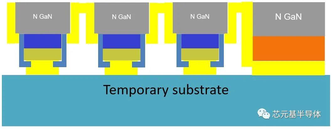
The breakthrough in technology by ChipFoundation Semiconductor on July 5, 2023,3, involves the use of chemical lift-off GaN from sapphire technique, along with a specially designed optical reflector and quantum dot color conversion technology. This breakthrough enables the production of high-efficiency, high-purity red light flip-chip quantum dot MiniLED chips and horizontal structure quantum dot MiniLED chips. The significant advancement is expected to effectively reduce the cost of red light chips, improve product cost-effectiveness, and potentially accelerate the commercialization process of quantum dot display technology.


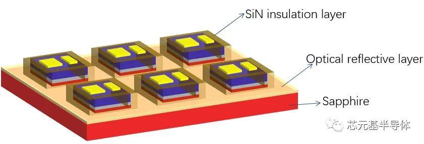
Figure 1: Structural schematic diagram
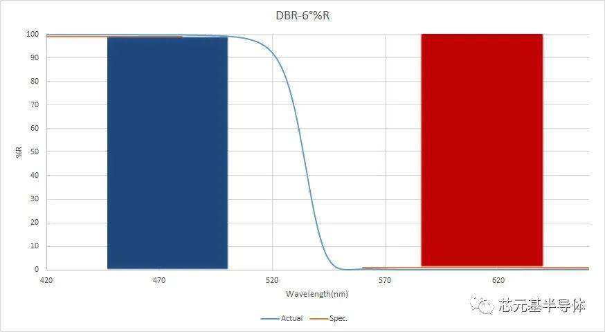
倒装结构量子点芯片技术方面,芯元基将剥离后的GaN芯片的出光面,用量子点胶水贴合到已经加工好的特殊光学反射层基板上,该光学反射层,对激发光源的波长具有高反射率,对量子点发光的波段具有非常高的透光率,以此来实现红光量子点更好激发,实现了红光量子点厚度小于1微米的情况下,量子点完全激发后,红光芯片无漏蓝光等现象。量子点芯片加工过程中,我们采用标准的半导体制程,结合光罩对准方法,在像素的侧壁做有高密度的介质层,实现量子点的完全密封,解决量子点在可靠度方面的顾虑。
In the flip-chip quantum dot chip technology, the chip substrate will lift off. ChipFoundation Semiconductor utilizes quantum dot glue to attach the light-emitting surface of the GaN chip to a pre-fabricated special optical reflection layer substrate. This optical reflector has a high reflectivity for the excitation wavelength of the light source and a very high transmittance for the emission wavelength of the quantum dot, thus achieving efficient excitation of the red light quantum dots. By doing so, the quantum dot thickness can be reduced to less than 1 micrometer while ensuring that the red light chip is fully excited without leakage of blue light or other phenomena. During the processing of the quantum dot chips, a standard semiconductor process is used, combined with mask alignment methods, to create a high-density dielectric layer on the sidewall of the pixel, achieving complete sealing of the quantum dots and addressing concerns about their reliability.

Figure 2: Optical Reflection Layer Design
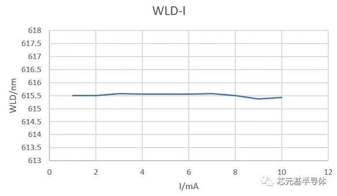
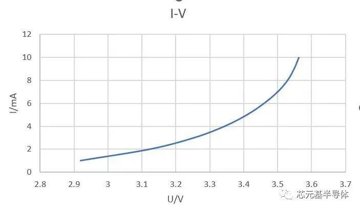
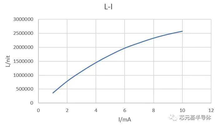
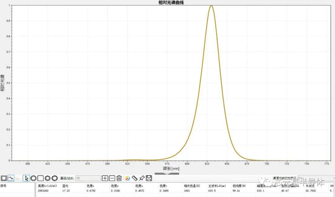
产品的特性曲线如下:(芯片尺寸:2*4mil/50*100um)

Forward Voltage Vs Forward current

Forward current Vs Relative Luminous Intensity

Forward current Vs Dominant Wavelength
|

|

|
 |
|
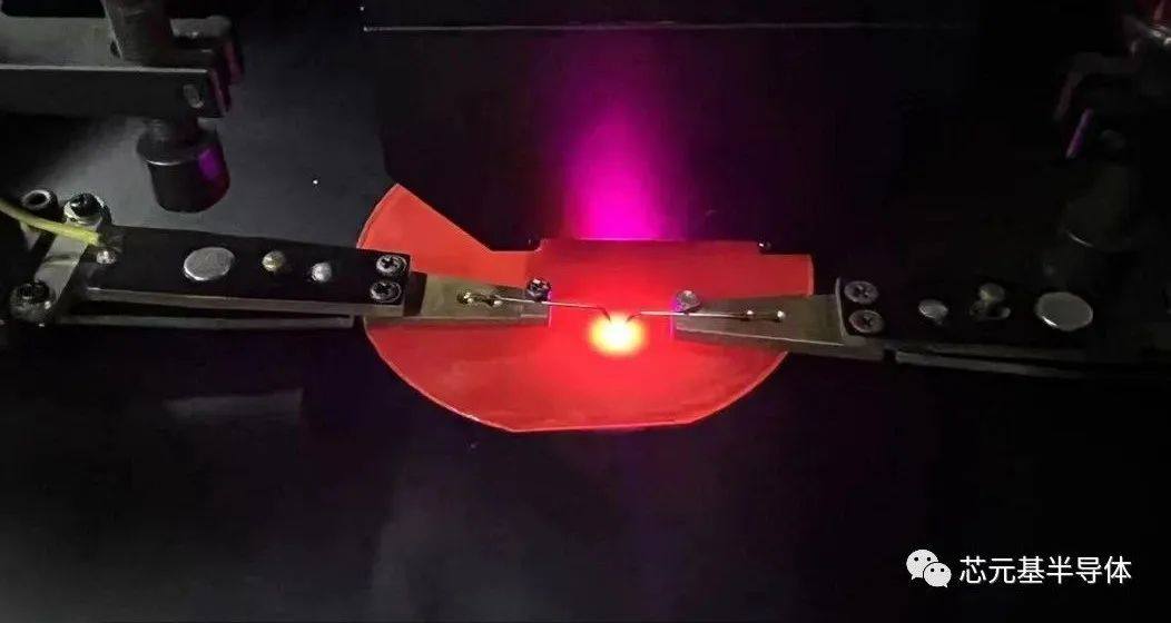
Schematic diagram of chip illumination
|
Flip-chip quantum dot MiniLED-Front illuminated image
|
Flip-chip quantum dot MiniLED -black illuminated image
|
|

|

|

|
|
Spectral distribution: no blue peak
|
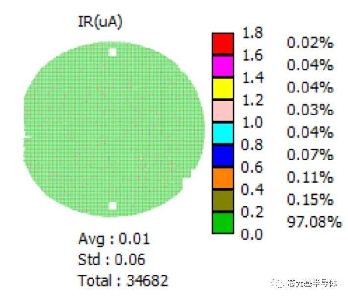
Chip leakage distribution: IR<0.1uA, yield greater than 97%
|
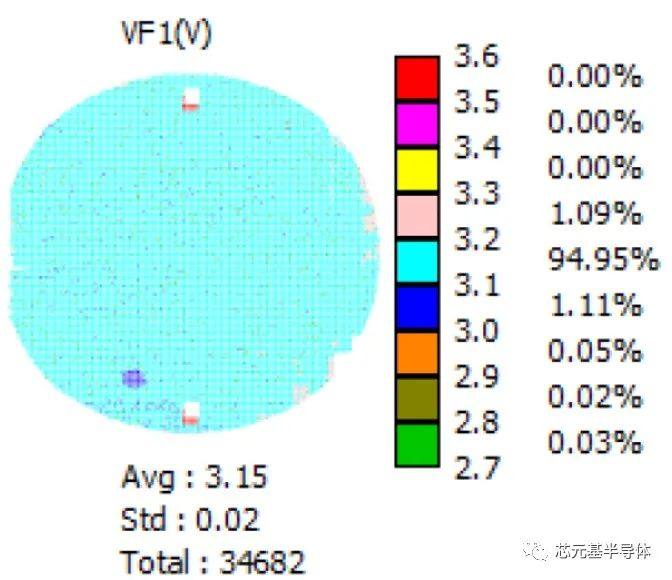
chip voltage distribution: 3.1-3.2V@5mA
|
后续,芯元基半导体将以此技术为基础,进一步开发与量子点色转换层相关显示器件技术,以达到未来高分辨率显示系统的实际需求。基于该量子点技术方案,芯元基半导体正在为国际知名机构开发尺寸小于0.2mm*0.2mm的量子点MIP器件。
In the future, ChipFoundation Semiconductor will further develop display device technologies related to quantum dot color conversion layers based on this technology to meet the practical requirements of high-resolution display systems.Based on this quantum dot technology scheme, ChipFoundation Semiconductor is currently developing quantum dot MIP(Micro LED in Package) devices with dimensions smaller than 0.2mm*0.2mm for internationally renowned institutions.
芯元基的量子点MIP技术,在GaN晶圆的每个子像素的侧壁均做有金属电极结构,这种结构除了有利于像素的共阴极设计外,也可以更好的解决独立子像素间的光串扰问题,在RGB量子点模板上(QDCC),采用特定结构设计的光学反射镜,实现红光、绿光的高效激发。所有的制程均采用标准的晶圆加工工艺,不需要巨量转移工艺,直接将晶圆芯片和QDCC模板键合,可更容易降低MIP的产业成本的同时,实现高可靠性的像素单元。
The ChipFoundation's quantum dot MIP technology has a metal electrode structure on the N-GaN sidewall of each sub pixel of the wafer . In the RGB quantum dot color conversion (QDCC) template, an optically reflective mirror with a specific structural design is used to achieve efficient excitation of red and green light. All processes are carried out using standard wafer fabrication techniques, eliminating the need for massive transfer processes. The wafer chip can be directly bonded to the QDCC template, making it easier to reduce the production cost of MIP while achieving high reliability of the pixel unit.

原文始发于微信公众号(芯元基半导体):芯元基实现高效纯红光量子点芯片,QD-Mini LED产品即将进入产业化阶段
